Jul
28
to Jul 29
The workshop will focus on the fundamentals of plasma etching and deposition. Lectures will include the basics of plasma reactors and mechanisms for etching and deposition and review state-of-the-art etching and deposition technologies as applied to semiconductor, MEMS, and nanofabrication. Talks will cover compound semiconductor, dielectric, and deep silicon etching as well as PECVD and high density plasma CVD of silicon based materials. Fundamental and new ideas for endpoint detection and sample thermal budget management will be presented.
To register for this event click here
Presented by Dr. Todd Hastings, Center for Nanoscale Science and Engineering (CeNSE) - U. of Kentucky
Join us for free pizza lunch @ UofL Shumaker Building Room 139
A new two-photon lithography system, the Nanoscribe Photonic Profession GT is now available at the CeNSE to all qualified users for both local and remote work.
The Nanoscribe is able to print structures with two stage modes: the “galvo mode” which allows much higher speed building, but with less precise features (~400 nm in 2D lateral resolution) compared to the more precise “piezo mode”, which has ~300 nm 2D lateral resolution. Feature sizes on the Nanoscribe range from roughly one hundred nanometers up to several millimeters, having a maximum build height of 3 mm. The available print area depends on the sample holder used. Learn more about this unique tool at our free “lunch & learn” seminar. Courtesy of KY Multiscale Nano Integration Node.

Dr. Chuang Qu
Post Doctoral Associate, KY Multi-Scale
Abstract
This talk focuses on two bottom-up approaches in nano-manufacturing: Microsphere Photolithography (MPL) and additive manufacturing of glass.The cost-effective manufacturing of two-dimensional metamaterials (metasurfaces) over large areas is a critical issue that limits their implementations. The first part of the talk introduces MPL process as a potential solution for the costly fabrication procedures. This talk discusses the fabrication capabilities, process control, and potential applications of MPL. MPL uses a scalable self-assembled microsphere array as an optical element to focus collimated light to nanoscale photonic jets in a photoresist layer. The concept is applied to the fabrication of metasurfaces with engineered IR absorption (e.g. perfect absorption with multiband/broadband and wavelength/polarization dependences).
The physics of feature formation in MPL is studied with a development model. The model enables the identification of fabrication conditions to improve the resolution and flexibility for the MPL process. The potential for a reusable microsphere array in MPL process is discussed as well. The use of the MPL for the fabrication of metasurfaces, with application such as sensing and thermal management, is novel as is the modeling of the MPL process.
Additive manufacturing has been used for printing metals, plastics, and ceramics. The second part of this talk will briefly introduce our work on additive manufacturing of optically transparent glass component using a new filament fed process. The process can be applied inprinting optical elements such as cylindrical lens and gradient index optics.
Bio
Dr. Chuang Qu received his BE and ME in Thermal and Power Engineering from Dalian University of Technology, China in 2012 and 2014, respectively, and Ph.D. in Mechanical Engineering from Missouri University and Science and Technology in 2019. He is currently a Postdoctoral Associate in the department of Speed School Electrical & Computer Engineering at the University of Louisville for the Kentucky Multi-Scale Manufacturing and Nano Integration Node (KY MMNIN). His research focuses on nanomanufacuting, additive manufacturing, and heat transfer. Emphasis has been on microsphere photolithography (MPL), with application to IR/optical sensing elements as well as for energy harvesting. He authored and co-authored 6 journal papers and 8 conference papers during his Ph.D study.
KY Multi-Scale Manufacturing and Nano Integration Node
Fiber lasers offer significant advantages for power scaling as compared with other laser system architectures. They provide a means for efficient pumping, improved heat management due to a large surface-to-volume ratio, excellent beam quality, high vibration tolerance, and established manufacturing techniques. During the past decades, we have worked to improve the fibers’ constituent core and cladding materials, to enable high-power optical isolators, and to enable other system components. However, new sensor approaches are needed as well. Traditional techniques for sampling the light in optical fiber sometimes require multiple splicing of fiber, are often time-consuming to employ, provide poor sensitivity, significantly perturb the fiber’s coupled light, and frequently lead to damage during higher-power fiber operation. We propose a new approach for fiber sensing that utilizes controlled Mie scattering from the fiber such that the detectors and fiber are mutually positioned by a Si microstructure. We recently demonstrated this approach as a way to quickly measure the attenuation of short-length high-loss optical fibers [Applied Optics 57 (2018)].
During the talk, high-power laser system architectures will be compared with an emphasis on the inherent advantages of fiber. The state-of-the-art for high-power fiber laser development will be outlined next with an emphasis on component needs. Finally, our recent effort to demonstrate a new means for characterizing optical fiber will be explained, and the potential of extending this approach to other components will be discussed.
Frank Kenneth Hopkins earned MS degrees in both electrical engineering and physics and a PhD degree in electrical engineering, all from the University of Cincinnati, and he completed Air War College. His professional career comprises several years of university teaching including three years at the University of Louisville, experience in industry including as a principal in the start-up of a public technology company, and greater than 31 years of federal service in the Air Force Research Laboratory and association with the Air Force Institute of Technology. Ken’s focus has been on materials and devices for laser sources, infrared detectors, and integrated photonics. His efforts led to the fielding of new airborne systems and thus to various awards including the Federal Laboratory Consortium Award for Excellence in Technology Transfer, the Meritorious Civilian Service Award, and the Technical Leadership Award from the Affiliate Societies Council of Dayton, Ohio. Ken is a Fellow of SPIE, a Senior Member of IEEE, and a member of the Assoc. of Old Crows. He has published more than 140 papers in various journals and conference proceedings, and he holds three patents.
Meeting Link: https://meetings.webex.com/collabs/#/meetings/detail?uuid=MDEGPHJ5IUXS0KJEO9KPQVO5KS-1BSR&rnd=881058.99096
Meeting Number: 198 347 779
Pranoy Deb Shuvra
Workshop Presenter
A major hurdle for space application is understanding the effect of radiation on MEMS devices. Although MEMS devices are believed to be more immune to radiation damage than their CMOS counterpart, this has not been studied in detail. We are investigating the radiation damage mechanism by radiating MEMS resonators with protons, UV radiation and x-ray radiation.

High aspect ratio free-standing MEMS resonator (655 um long, 2 um wide and 15um thick)

Close up of a 900nm wide MEMS resonator
This talk will focus on the fabrication of micro-resonators that are fabricated in the University of Louisville’s state of the art cleanroom facility. Silicon-on-Insulator (SOI) wafers are used for this three-mask fabrication process. At the last step of fabrication, the sacrificial buried oxide is dissolved using the recently acquired anhydrous HF vapor etch system. The HF vapor etch provides much more flexibility and much better yield compared to the BOE (buffered oxide etch) release of MEMS resonators.
Pranoy Deb Shuvra is a PhD candidate in the Electrical and Computer Engineering Department of the Speed School of Engineering at the University of Louisville. He is working on the design, simulation, fabrication and testing of microelectromechanical system (MEMS) devices for last five years. He fabricates MEMS devices at the University of Louisville’s MNTC cleanroom facility. His current project is to understand the effect of radiation on MEMS devices. This project is funded by DTRA (Defense Threat Reduction Agency). He has published in JMM, IEEE Transaction on Nuclear Sciences, and Physical Review Applied.
Dr. Sven Cremer
“Neuroadaptive Human-Machine Interfaces for Collaborative Robots”
With an increasing number of collaborative robots or “co-robots” entering human environments, there is a growing need for safe, intuitive, and efficient (physical) Human-Machine Interfaces. Unlike industrial robots, co-robots operate in cluttered and dynamic working spaces where accidental collisions may occur. To minimize interaction forces, co-robots are usually lightweight and compliant. However, this makes the robot dynamics highly nonlinear and therefore difficult to control. In addition, the control loop must incorporate feedback from integrated sensors. Future systems under development are covered with force-sensing robot skin consisting of thousands of multi-modal sensors, creating the need for efficient robot sensor calibration and processing.
During this work, a neuroadaptive (NA) controller was developed and validated for safe and stable physical interaction. In order to achieve intuitive physical Human-Robot Interaction (pHRI), the robot error dynamics were modified to behave equivalent to a simple admittance model by expanding the NA controller with Prescribed Error Dynamics (PED). Another developed approach for modifying the robot error dynamics was an inner/outer-loop structure consisting of an admittance model in the outer-loop, which generates a model trajectory that the inner-loop follows. This admittance model was implemented with an autoregressive-moving-average (ARMA) filter, which was tuned with recursive least squares and by using a prescribed task model. Experiments conducted showed that the developed framework allows a high degree of generality and adaptability to different human preferences, tasks, robots, and sensors. It is also offers a novel algorithm for adaptive calibration of robot skins by directly tuning admittance models that map sensor voltages into desired robot motion. Finally, it was suggested that the pHRI can be made more efficient by reducing the human effort during a collaborative task. The human force exerted on the robot to achieve a desired pose can be minimized by predicting and then executing the desired human motion. Different Human Intent Estimators (HIEs) were proposed, including a neural network based estimator.
Sven Cremer was born near Köln, Germany and grew up in Göteborg, Sweden. He received his B.Sc. degree in Engineering Physics and Applied Mathematics from the University of the Pacific, California, in 2010. Because of his passion for robotics, he pursed a Ph.D. degree in Electrical Engineering with a focus on control systems at The University of Texas at Arlington. In 2013, he joined the Next Generation Systems (NGS) group headed by Professor Dan O. Popa and worked on projects involving human-machine interfaces, assistive robotics, neuroadaptive control, and robot skin.

Dr. Oguz Yetkin
EMG-Free Control Strategies for Low Cost 3D Printed Robotic Prosthetics
Abstract
Control of robotic prosthetic devices is typically achieved through electromyogram (EMG) signals read from the residual limb. While this is the state of the art, it has several disadvantages including cost, unavailability of residual muscles for some patients, and the ability to control only a single degree of freedom (DOF) at a time.
We have re-framed the prosthetic control problem as a Human Robot Interface problem and developed several robotic interface methods which can eliminate or complement the use of EMG signals while allowing the user to quickly achieve more grasping patterns, thus allowing the use of all the DOFs available in the prosthetic device.
This talk will discuss the methods developed, as well as on-going work focusing on their adaptation into an easily deployable, low cost 3D printed robotic prosthetic system.
Biography
Dr. Oguz Yetkin, Ph.D. is a biomedical engineer and a Visiting Scientist at Ege University. He obtained his Ph.D. degree from University of Texas at Arlington in Bioengineering after developing a human-robot interface system for controlling prosthetic devices while working with the Next Generation Systems lab with Dr. Dan Popa.
Dr. Yetkin also holds a B.S. degree from the University of Wisconsin-Madison in Molecular Biology and Computer Science. Dr. Yetkin has more than a decade of experience as a professional software engineer and systems integrator. Dr. Yetkin’s areas of expertise include data visualization, algorithm development, medical imaging, prosthetic device control, computer-human interfaces, microfabrication, and rapid prototyping of new technologies.
Design and Activation of Nanoparticles for Cancer Therapy
Renat R. Letfullin
Department of Physics and Optical Engineering
Rose-Hulman Institute of Technology
Tuesday, February 28th, 2017, 11:00 am – Noon
University of Louisville Shumaker Research Building, Room 139
Refreshments will be served.
Presented will be an overview of recent scientific and engineering advances in nanomedicine and its current and potential applications. The interaction between nanoparticles and radiation holds great interest and promise in nanomedicine, introducing such possibilities as selective cell targeting by nanoparticles to create highly localized thermal cell damage. We will discuss the design and methods of activation of nanodrugs selectively delivered to the tumor site, with new dynamic modes in selective nanophotothermolysis of cancer.
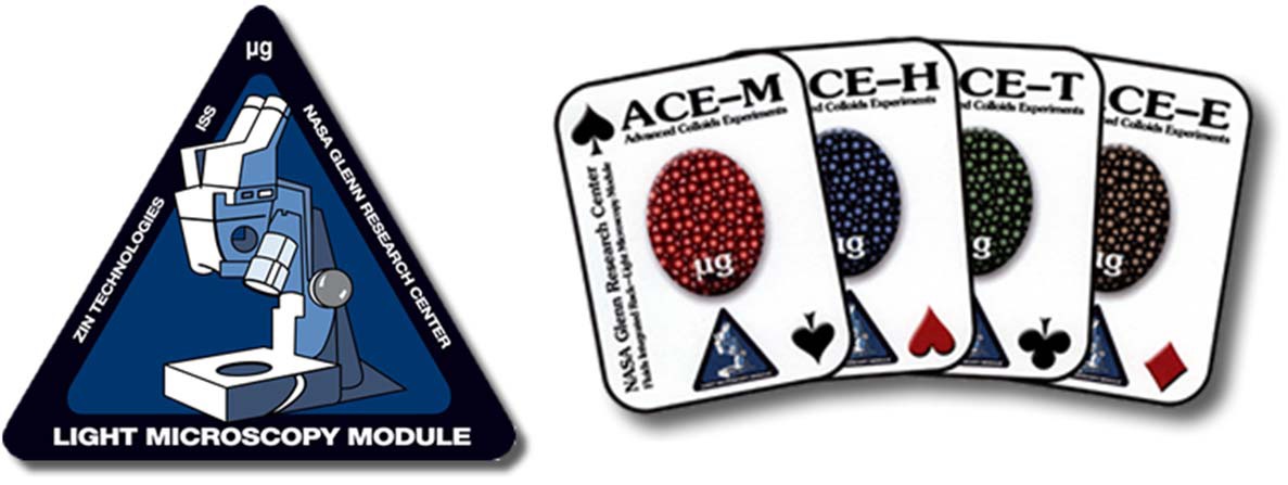
Guest Speaker: Bill Meyer
From: Advanced Research Associates (USRA), NASA Glenn Research Center
Refreshments will be provided
Friday, February 3rd, 10:00am
Shumaker Research Building, Room 139

A brief (and selective) overview of NASA’s microgravity colloids program will be
shared. This will consist of some of the science highlights and the techniques used to obtain them. Part of this presentation will include recent and planned microgravity colloids research with the Kentucky science teams (Professors Stuart Williams, Gerold Willing, and Hemali Rathnayake) led by the University of Louisville.
Time allowing, this presentation will culminate with a short movie showing the hand-off of the Janus particles presently being studied on the International Space Station (ISS), along
with “inside” film footage showing the supporting launch and landing of the SpaceX-9 rocket that delivered this experiment to the ISS.
DR. KENG H. HSU
ASSISTANT PROFESSOR OF MECHANICAL ENGINEERING
ARIZONA STATE UNIVERSITY
UofL Host: Thomas Berfield, tom.berfield@louisville.edu. Office ph:502-852-7173
Abstract: Large-scale production of complete systems and complex end-use products in
one setting on one platform is the Holy Grail of additive manufacturing. Major
breakthroughs in the understanding of how to manipulate physical, chemical, and material science principles to harness materials-energy interaction for manufacturing need to be made to enable engineering of existing and new material processing techniques to be developed to advanced towards that ultimate goal. In this talk, several new materials processing techniques are introduced wherein metals, polymers, and ceramics can potentially be co-printed in the same process domain to allow multi-material 3D printing of complete systems. Challenges in these processes and the fundamental questions at the core of these processes will be discussed
Biography: Dr. Keng Hsu is an Assistant Professor at Arizona State University’s Ira A.
Fulton Schools of Engineering. Since 2013, Dr. Hsu has directed the Advanced Mult-scale
Manufacturing Lab at Arizona State. There, his research has focused on addressing the need for new manufacturing processes at the nano-, micro-, and meso-scales required to bring theoretical materials to reality. This highly interdisciplinary research leverages principles in physics, chemistry, and mechanics and solve engineering problems along the way. Current research projects by Dr. Hsu include Photoconduction-Induced Localized
Electrochemical Deposition for Metal 3-D Printing, Thermal-Acoustic 3D Printing of
Polymer-Metal Composites, Scalable Electrochemical Patterning of Semiconductors, Design, Fabrication, Characterization, and Tuning Of Plasmonic Structures for Bio-Sensing, Optical Devices, And Energy Conversion Applications, and Design for Additive Manufacturing.
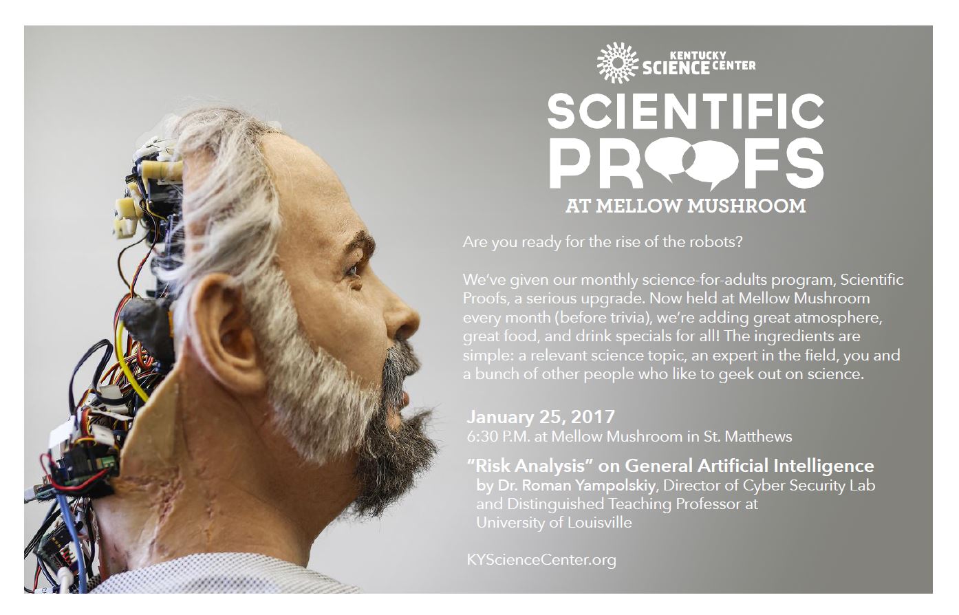
Are you ready for the rise of robots?
KY MMNIN collaborations with the Kentucky Science Center proudly announces this event:
KSC has given their monthly science-for-adults program, Scientific Proofs, a serious upgrade. Now held at Mellow Mushroom in St. Mathews, KY.
On January 25, 2017 @ 6:30PM two presentations will take place:
"Risk Analysis" on General Artificial Intelligence by Dr. Roman Yampolskiy, Director of Cyver Security Lab and Distinguished Teaching Professor at University of Louisville
Robotic demonstration by Dr. Indika Wijayasingue, Research Associate, Next Generation Systems Group headed by Prof. Dan Popa, Department of Electrical and Computer Engineering, UofL.
The Kentucky Multiscale-Manufacturing NNCI Site, UofL Dept. of Electrical and Computer Engineering, and the Speed Research and Scholarship Committee are honored to jointly sponsor this seminar.
by Philip Feng, Ph.D. - Electrical Engineering, Case School of Engineering, Case Western Reserve University
Atomically-thin crystals derived from new classes of layered materials have rapidly emerged to enable two-dimensional (2D) nanostructures with unusual electronic, optical, mechanical, and thermal properties. While graphene has been the forerunner and hallmark of 2D crystals, newly emerged compound and single-element 2D semiconductors offer intriguing attributes beyond graphene’s (e.g., including sizeable and tunable bandgaps covering a wide spectrum with technological importance). In this talk, I will describe my research group’s latest efforts on investigating how mechanically active atomic-layer semiconducting nanostructures interact with optical and electronic interrogations, and on engineering such structures into ultrasensitive transducers and ultralow-power signal processing building blocks. I will show the demonstrations of highly tunable multimode resonant 2D nanoelectromechanical systems (NEMS) and vibrating-channel transistors using single-layer and few-layer transition metal di-chalcogenides (TMDC), with both optical and electrical readout. I will describe spatially mapped mode shapes and Brownian motion detection in these atomic-layer multimode nanoresonators at room temperature, along with the device physics and coupling effects that govern the signal transduction. I shall then demonstrate black phosphorous 2D devices that exploit the crystal’s unique and strong intrinsic anisotropy. Finally, I will discuss the potential toward emerging applications, including ultrasensitive detection in fundamental studies, ultralow-power transducers, and 2D nanosystems.
Short Bio
Philip Feng is currently an Associate Professor in Electrical Engineering at Case School of Engineering, Case Western Reserve University (CWRU). His group’s research is primarily focused on emerging nanoscale devices and integrated microsystems. He received his Ph.D. from Caltech in 2007 for developing ultra high frequency (UHF) nanoelectromechanical systems (NEMS) with low-noise technologies for real-time single-molecule sensing. His recent awards include a National Science Foundation CAREER Award, 3 Best Paper Awards (with his advisees, at IEEE NEMS 2013, IEEE Int. Freq. Control Symp. 2014, and AVS Int. Symp. 2014) out of 8 nominated Finalists for Best Paper Award Competitions, and a university-wide T. Keith Glennan Fellowship. He is also the recipient of the Case School of Engineering Graduate Teaching Award (2014) and the Case School of Engineering Research Award (2015). He was one of the 81 young engineers selected to participate in the National Academy of Engineering (NAE) 2013 U.S. Frontier of Engineering (USFOE) Symposium. Subsequently, he was selected to receive the NAE Grainger Foundation Frontiers of Engineering (FOE) Award in 2014 (two recipients in the nation). He has served on the Technical Program Committees (TPC) for IEEE IEDM, MEMS, Transducers, IFCS, and other conferences, and is the TPC Chair for the American Vacuum Society (AVS) MEMS/NEMS group and program. He is a Senior Member of IEEE, and a member of APS and AVS.
Related References:
1. Wang, Jia, Feng, et al., “Resolving and Tuning Mechanical Anisotropy in Black Phosphorus …”, Nano Lett. 16, 5394-5400 (2016).
2. Lee, Wang, Feng, et al., “High Frequency MoS2 Nanomechanical Resonators”, ACS Nano 7, 6086-6091 (2013).
3. Wang, Lee, Feng, “Spatial Mapping of Multimode Brownian Motions…”, Nature Communications 5, 5158 (2014).
4. Yang, Islam, Feng, “Electromechanical Coupling & Design Considerations in Single-Layer…”, Nanoscale 7, 19921-29 (2015).
5. Yang, Zheng, Feng, et al., “Multilayer MoS2 Transistors Enabled by a Facile Dry-Transfer Technique…”, Journal of Vacuum Science & Technology B 32, 061203 (2014). (Cover Article, Editor’s Pick, ‘Most Read’ of the Month)
6. Wang, Jia, Feng, et al., “Black Phosphorus Nanoelectromechanical Resonators…”, Nanoscale 7, 877-884 (2015).
7. Yang, Wang, Feng, et al., “Electrical Breakdown of MoS2 Transistors…”, Nanoscale 6, 12383-12390 (2014).
8. Wang, Lee, Feng, et al., “Embracing Structural Nonidealities in 2D…”, Scientific Reports 4, 3919 (2014).
Invited guest speaker: Dr. F. Kenneth Hopkins, Principal Electronics Engineer for the Air Force Research Laboratory (AFRL)
The mid-infrared spectral region, extending from a wavelength of 3 to 5 μm, has been extensively used by the military since the 1950’s, but it also offers a number of non-military laser applications such as differential absorption lidar systems for helicopter-based petroleum exploration and pipeline monitoring. In addition, laser system requirements on an aircraft are the same as those preferred for commercial products such as lasers purchased for use in medical offices. These include a system that is generally benign for workers with long times between refueling or maintenance events, relatively compact in size and weight, efficient to reduce cooling and power requirements, and able to withstand abuse such as from mechanical shock and vibration. Higher power mid-IR laser radiation is required for many applications.
In the talk, the various approaches for constructing mid-IR lasers will be described along with their advantages and limitations, and these will be compared with regard to their ability to scale-up average output power. The discussion will include a review of the published state-of-the-art, and a description of the basic physics that presently limit each approach. There are several areas of specific interest. First, the chalcopyrite semiconductor, CdSiP2, a nonlinear optical (NLO) crystal for shifting laser power from shorter-wavelengths into the mid-IR, was identified by this author as the most promising NLO crystal for scale-up, but it is presently limited by various crystal defects that we are characterizing and developing techniques to control. Second, new materials are emerging for semiconductor laser diodes that offer high-risk/high-payoff rewards, along with new approaches for coherent combining of quantum cascade lasers. In addition, Fe:ZnSe, a material that we investigated many years ago, continues to be of interest to this author as development progresses slowly but steadily worldwide.
Bio:
F. Kenneth Hopkins is a Principal Electronics Engineer for the Air Force Research Laboratory (AFRL) where he has investigated and developed photonic materials during the past 30 years. Concurrently, he is an Adjunct Professor at the Air Force Institute of Technology. Prior to AFRL, Dr. Hopkins taught in universities and worked in industry including serving as a principal officer in a new photonics start-up company that successfully went public. He is a Fellow of the International Society for Optics and Photonics (SPIE), and a member of IEEE and AOC. His successful past efforts have directly led to the fielding of airborne systems and thus to various awards including the Meritorious Civilian Service Award, the Outstanding Engineers and Scientists Award from the Affiliate Societies Council of Dayton, Ohio, and the Federal Laboratory Consortium Award for Excellence in Technology Transfer. Dr. Hopkins has authored more than 125 publications and holds 3 patents. He earned both PhD and MS degrees in electrical engineer and a MS degree in physics, all from the University of Cincinnati. His BS degree in physics and mathematics was from Northern Kentucky University.
A Seminar Sponsored by KYMULTISCALE.NET\
NEXT GENERATION SYSTEMS GROUP
DEPARTMENT OF ELECTRICAL AND COMPUTER ENGINEERING
SPEED SCHOOL OF ENGINEERING
SHUMAKER RESEARCH BLDG ROOM 139
2210 SOUTH BROOK ST. LOUISVILLE, KY 40208

Conn Center for Renewable Energy Research &
The Micro/Nano Technology Center
are pleased to host
Dr. Larry Holloway
State Director, Kentucky DOE EPSCoR
University of Kentucky
Kentucky DOE EPSCoR: Growing Energy Research and Collaborative Networks in Kentucky
Presentation & Discussion
Friday, March 11, 9:00 – 10:00 AM
Ernst Hall Room 212
The DOE-EPSCoR program is a program of the US Department of Energy to stimulate competitive research in selected states. The state KY-DOE-EPSCoR program is responsible for coordinating submissions from the state of Kentucky to the national DOE EPSCoR program, and more broadly for encouraging competitive energy-related research in Kentucky.
At the beginning of this seminar, a brief presentation will overview the national DOE EPSCoR program and the goals of the KY-DOE EPSCoR program to grow more energy-related research in the state. After the presentation, the seminar will move to a discussion format. Attendees will be asked to introduce themselves and briefly summarize their research areas. A discussion will then consider ways the KY-DOE EPSCoR program can encourage collaborative energy-related research networks and facilitate more competitive energy-related research activity in the state.
Biography: Larry Holloway is State Director of Kentucky DOE EPSCoR. He also is Director of the University of Kentucky Power and Energy Institute (PEIK), a program created through a series of grants from the US Department of Energy. He currently serves as chair of the Department of Electrical and Computer Engineering, and was formerly the Director of the UK Center for Manufacturing. He received his BS degree from Southern Methodist University and his Masters and PhD degrees from Carnegie Mellon University.

a site of the National Nanotechnology Coordinated Infrastructure (www.nnci.net)
ACKNOWLEDGMENT OF SUPPORT AND DISCLAIMER
This material is based upon work supported by the National Science Foundation under Grant No. 2025075. Any opinions, findings, and conclusions or recommendations expressed in this material are those of the author(s) and do not necessarily reflect the views of the National Science Foundation.